




 Castaways Bistro: Punta Cana Paradise
Home»Business»SK Hynix Commits More Than $4 Billion to Indiana AI Memory Facility
SK Hynix Commits More Than $4 Billion to Indiana AI Memory Facility
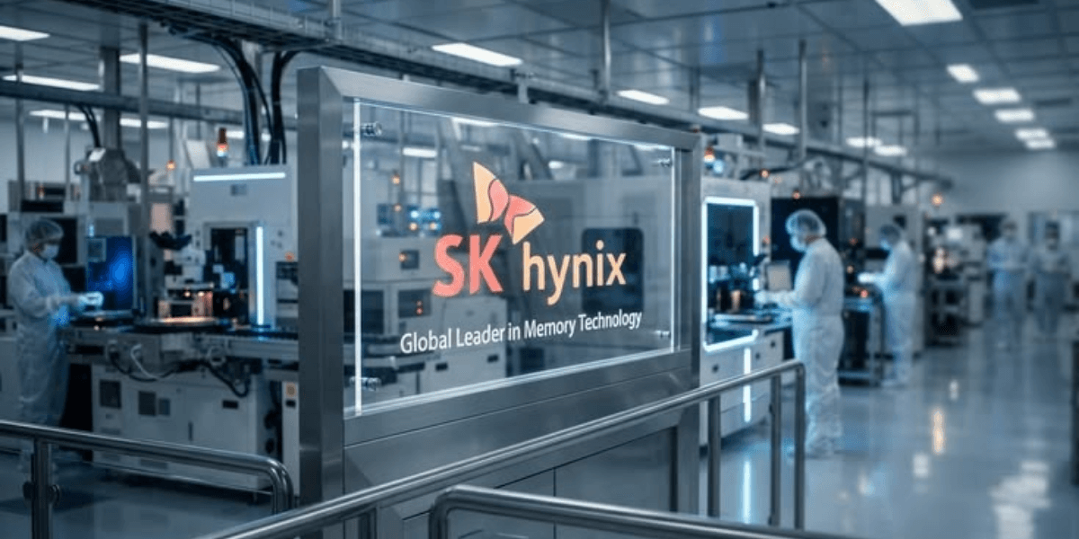
SK Hynix broke ground Thursday on a major Indiana semiconductor facility that will expand the company's U.S. manufacturing presence and strengthen the supply chain supporting artificial-intelligence computing.
The South Korean chipmaker said it plans to invest more than $4 billion in an advanced packaging and research facility at Purdue Research Park in West Lafayette. The project is designed to produce high-bandwidth memory, or HBM, used in advanced AI systems.
The company expects the Indiana operation to begin volume production of its next-generation HBM4E memory in the third quarter of 2029.
SK Hynix Chief Executive Kwak Noh-Jung said the company expects the current global memory shortage to persist through 2030, reflecting the strength of demand generated by AI infrastructure investment.
The project represents a strategic expansion rather than simply a new manufacturing site.
HBM is a specialized type of memory designed to move large amounts of data quickly between processors and memory. It has become particularly important in AI computing because advanced accelerators require substantial memory bandwidth to train and operate increasingly complex models.
The growth of generative AI has therefore created demand not only for processors but also for the memory technologies surrounding them.
SK Hynix is one of the world's largest HBM suppliers and has established relationships with major technology companies, including Nvidia, Google and Microsoft. The Indiana facility is intended to bring part of that supply chain closer to U.S. customers.
For business leaders, the project illustrates how AI is influencing capital allocation across the semiconductor industry.
Companies that once focused primarily on traditional computing demand are now expanding production capacity to support AI data centers, cloud infrastructure and specialized computing systems.
The scale of SK Hynix's investment also demonstrates the long planning cycles involved in semiconductor manufacturing.
The facility will not begin next-generation HBM4E production for several years, meaning the company is making a substantial capital commitment based on expectations about future demand.
That strategy carries both opportunities and risks.
If AI infrastructure spending remains strong, additional memory capacity could help address supply constraints and provide SK Hynix with greater access to the U.S. market.
If demand changes significantly, however, semiconductor companies can face periods in which expensive facilities operate below capacity.
SK Hynix's executives have indicated that they currently see continued demand rather than a near-term downturn.
The Indiana project is also part of a broader American effort to strengthen domestic semiconductor supply chains.
The company said the facility is expected to create approximately 7,000 direct and indirect jobs and support an ecosystem involving more than 100 partners. The project is also supported by federal funding under the CHIPS Act, including grants and potential loans.
The facility will include an advanced packaging production line, cleanroom capabilities and research facilities.
SK Hynix is also working with Purdue University on research and development involving next-generation advanced packaging technology.
That university connection provides a workforce and research component to the project.
Semiconductor companies require engineers, technicians, researchers and manufacturing specialists, making partnerships with universities increasingly important as the industry expands.
The Indiana facility also reflects the growing importance of advanced packaging.
Traditional semiconductor manufacturing often receives most of the public attention, but packaging is increasingly important because it determines how chips and memory components are connected and integrated into high-performance computing systems.
For AI infrastructure, the ability to package memory and processors efficiently can influence system performance, power consumption and overall computing capacity.
The project therefore addresses several business challenges simultaneously: supply-chain resilience, manufacturing capacity, workforce development and proximity to major technology customers.
Its location in Indiana also broadens the geographic footprint of America's semiconductor industry beyond traditional technology centers.
SK Hynix has indicated that the Indiana site will become its first U.S. hub for next-generation HBM production.
The broader strategic significance is that AI is changing where semiconductor companies invest and what types of facilities they build.
As demand for AI computing expands, memory has become a critical component of the technology supply chain.
The West Lafayette project gives SK Hynix a larger U.S. presence while providing another major investment in America's semiconductor manufacturing infrastructure.
For business leaders, the development offers a clear example of how technological shifts can translate into multibillion-dollar industrial decisions.
The facility will not begin full-scale production immediately, but Thursday's groundbreaking marks the beginning of a long-term investment designed around the expectation that AI computing will remain a major driver of semiconductor demand.

Leadr Magazine Contributor
Ashley Franklin
Covers entrepreneurship, branding, leadership, and emerging companies.
This article features partner, contributor, or branded content from a third party. Members of the Leadr Magazine editorial staff were not involved in the creation of this content. All views and opinions are those of the contributor alone.
Related Posts
Castaways Bistro: Punta Cana Paradise The Revenue Hiding in Your Business Back End
 Vallejo Relief Center: Highway 80's Cultural Hub